A solar panel generates electricity using the photovoltaic effect, a phenomenon discovered in 1839 when Edmond Becquerel, a French physicist, observed that certain materials produced an electric current when exposed to light. Two layers of a semi-conducting material are combined to create this effect. One layer has to have a depleted number of electrons. When exposed to sunlight, the layers of material absorb the photons. This excites the electrons, causing some of them to ‘jump’ from one layer to the other, generating an electrical charge.
There are two methods for converting solar power into electricity, thermal which is based on concentrating solar power by mirrors or other type of reflectors to produce high temperature to generate water vapour or other liquids with high pressure to rotate turbines to generate electricity or by making use of photovoltaic (PV) effect to convert solar power to electric power directly. Photovoltaic technology operates by catching the photons of light and manipulating them to produce free electrons. These electrons generate an electric current. The main way to develop this technology is through solar power panels or PV cells. A PV cell is a semi-conductor cell which is able to convert solar rays into electrical power.
There are three main steps a solar cell undergoes. First step, the photons in the form of sunlight hit the solar cell, which is covered by the semiconductor silicon. When a photon hits a piece of silicon, one of three things can occur depending on the energy in the photon: either the photon reflects off the surface, the photon passes through the silicon, or the photon is absorbed by the silicon.
Photovoltaic Solar Cell Construction
Photovoltaic cells consist, in essence, of a junction between two thin layers of dissimilar semiconducting materials, the first is made of silicon doped with small amount of phosphorus which has one more electron in its outer orbital than silicon. When a phosphorus atom takes place of a silicon atom, the extra electron is transferred to the crystal lattice. As these electrons with negative charge are free to move, so this material is known as n-type silicon. P-type silicon gets its positively charged particles from tiny amounts of boron, an element that has one less electron than silicon in its outer shell.
In this case there are not enough electrons to form all the covalent bonds required, so the electrons move around to try to fill this deficiency, which is called a hole. Holes act like free, positively charged particles. When p-type and n-type materials are placed together, they form a p-n junction as shown in Figure.1. Electrons and holes attract each other, congregate by the interface, and leave the p-type and n-type regions with negative and positive charges, thus creating the required electric field.
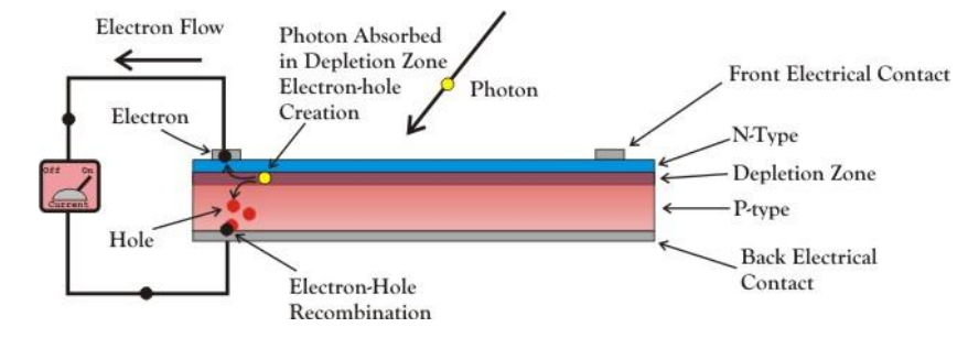
When light shines on crystalline silicon, electrons within the crystal lattice may be freed. But not all photons, as packets of light energy are called, are created equal. Only photons with a certain level of energy can free electrons in the semiconductor material from their atomic bonds to produce an electric current. This level of energy, known as the “bandgap energy,” is the amount of energy required to dislodge an electron from its covalent bond and allow it to become part of an electrical circuit. To free an electron, the energy of a photon must be at least as great as the bandgap energy.
However, photons with more energy than the bandgap energy will expend that extra amount as heat when freeing electrons. Crystalline silicon has a bandgap energy of 1.1 electron-volts (eV). (An electron-volt is equal to the energy gained by an electron when it passes through a potential of 1 volt in a vacuum.) The bandgap energies of other effective PV semiconductors range from 1.0 to 1.6 eV as shown in figure below. In this range, electrons can be freed without creating extra heat.
| semi-conductor | density [g/cm3] | Z | Egap [eV] | ϵ [eV] | X0 [cm] |
| Si | 2.33 | 14 | 1.12 | 3.6 | 9.37 |
| Ge | 5.33 | 32 | 0.67 | 2.9 | 2.30 |
| CdTe | 5.85 | 48,52 | 1.44 | 4.43 | 1.52 |
| CdZnTe | 5.81 | 1.6 | 4.6 | ||
| HgI2 | 6.40 | 80,53 | 2.13 | 4.2 | 1.16 |
| GaAs | 5.32 | 31,33 | 1.42 | 4.3 | 2.29 |
Table 2.3.1 showing band gap energies of other PV semiconductors
Egap: band gap energy
ϵ : an ionization potential
X0: radiation length
Factors that Affect Efficiency of Solar Cells
Five major factors affect the performance output of photovoltaic panels, also the PV technology is widely used in ATO solar generators, those five factors including load resistance, sunlight intensity, cell temperature, shading and crystalline structure.
Load Resistance: The characteristic resistance of a solar cell is the output resistance of the solar cell at its maximum power point. If the resistance of the load is equal to the characteristic resistance of the solar cell, then the maximum power is transferred to the load and the solar cell operates at its maximum power point. For the batteries to charge, the panels must operate at a slightly higher voltage than the battery bank voltage. PV systems’ application should at voltages close to the maximum power point of the array. If a load’s resistance is well matched to a panel’s I-V performance, the panel will operate at or near the maximum power point, resulting in highest possible efficiency. As the load’s resistance increases, the panel will operate at voltages higher than the maximum power point, causing efficiency and current output to decrease.
Temperature: Solar cells generally work best at low temperatures. Higher temperatures cause the semiconductor properties to shift, resulting in a slight increase in current, but a much larger decrease in voltage. Extreme increases in temperature can also damage the cell and other module materials, leading to shorter operating lifetimes. Since much of the sunlight shining on cells becomes heat, proper thermal management improves both efficiency and lifetime.
Sunlight Intensity: Changing the light intensity incident on a solar cell changes all solar cell parameters, including the short-circuit current, the open-circuit voltage, the FF, the efficiency and the impact of series and shunt resistances. The light intensity on a solar cell is called the number of suns, where 1 sun corresponds to standard illumination at AM1.5, or 1 kW/m2. For example a system with 10 kW/m2 incident on the solar cell would be operating at 10 suns, or at 10X. A PV module designed to operate under 1 sun conditions is called a “flat plate” module while those using concentrated sunlight are called “concentrators”.
Shading: Shading can have a huge impact on the performance of solar photovoltaic panels. Solar generator with solar panels consist of a number of solar photovoltaic cells wired together into a series circuit this means that when the power output of a single cell is significantly reduced, the power output for the whole system in series is reduced to the level of current passing through the weakest cell. Therefore, a small amount of shading can significantly reduce the performance of your entire solar photovoltaic panels system.
Crystalline Structure: Polycrystalline have a surface with a random pattern of crystal borders rather than the solid colour of single-crystal cells. Since a low-cost silicon is used to fabricate polycrystalline cells, their efficiency is typically in the range of 12%-14%, a value slightly less than the monocrystalline cells, but much higher than solar technologies such as thin film. While monocrystalline silicon features upstanding randomly distributed pyramids, the surface of multicrystalline silicon solar cells mostly features a randomly distributed order of round shaped valley. Main functions of the texture are to increase transmission of incoming photons into the silicon absorber and increase the path length of the photons inside the absorber (oblique direction of the photon propagation relative to the surface and high internal reflection surfaces).
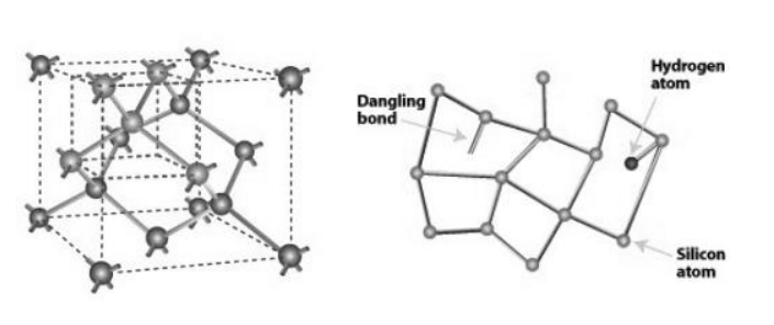
Both types of silicon, c-Si and a-Si, can be doped with phosphorus and boron to create P-type and N-type layers of silicon. Because a-Si can have more concentrated silicon randomly bonded together, a-Si layers can be much thinner than c-Si. This causes solar cells made of aSi to be very thin and flexible.