RESEARCH DIRECTIONS
Solar Photon Converters
The traditional approach to development of new materials for application in photovoltaics has been to identify materials developed for other technological purposes and assess their suitability to adaptation in photovoltaics. Thus, the materials themselves were developed for other purposes, and their development often follows the basic sequence in which (1) an interesting property is discovered; (2) a useful application is invented; (3) “basic research” starts; and (4) development occurs until the material is of adequate quality for the identified application.
A shortcoming of this approach is that the discovery process relies on accident or serendipity, or targeting in a limited domain, and ultimate success requires a long research and development process. A more desirable approach is one that emphasizes design of materials with targeted properties as an integral part of the discovery process (see Figure 1). New approaches to discovery-by-design can be based on several observations:
- Current research-oriented advanced materials synthesis and processing methods can produce a wide variety of both equilibrium and nonequilibrium atomic configurations — almost at will.
- The choice of atomic configuration in a material controls many of its physical properties.
- There are often too many possible atomic configurations for direct and explicit prediction of properties.
Thus, the challenge underlying these observations is to identify an atomic configuration (structure) with a given, useful target property, out of an astronomical number of possibilities. Progress in both theoretical and experimental methods is needed. For photovoltaics and photoelectrodes, the materials properties that need to be identified and optimized include semiconductor band structure, band gap, band edge energies, carrier mobilities, electron affinity, work function, oscillator strength and selection rules (direct vs indirect band gap), phonon spectrum, electron-phonon scattering parameters, lattice constants, atomic order-disorder behavior, and defect structure. The specific properties required will depend upon the specific type of device being considered.
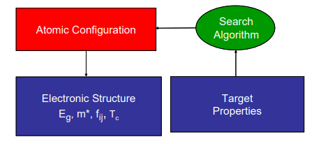
Figure 1 Materials by design. In one manifestation, the process begins with a set of target properties. A simulation tool is combined with a search algorithm process to find a test atomic configuration, then calculates the values of the properties and adjusts the configuration if necessary. The loop is repeated until the calculated properties match the target input.
Thermoelectrics
Comprehensive Theoretical Guidance on Thermal and Electronic Transport in Complex Structures. Over the past decade, progress has been made in the theory of thermoelectricity, noticeably the work of quantum size effects on the electronic power factor, interface effects on the thermal conductivity, and the use of density functional theory for the electron and phonon band structures. However, existing theoretical approaches lack predictive power. For bulk materials, the challenges lie in predicting the structures of materials, and their electronic and phononic band structures and transport properties, and in understanding the impact of defects in the materials on Atomic Configuration Electronic Structure Eg, m*, fij, Tc Target Properties Search Algorithm Atomic Configuration Electronic Structure Eg, m*, fij, Tc Target Properties Search Algorithm Figure 55 Materials by design. In one manifestation, the process begins with a set of target properties. A simulation tool is combined with a search algorithm process to find a test atomic configuration, then calculates the values of the properties and adjusts the configuration if necessary. The loop is repeated until the calculated properties match the target input. For nanostructured materials, a crucial issue is the role of interfaces on electron and phonon transport. Although the ultimate goal should be set at predictive tools, modeling should help in pointing directions for materials synthesis and structural engineering. Insights gained through combined theoretical and experimental studies on fundamental thermoelectric transport processes are invaluable in the search of materials with high values of ZT, the thermoelectric figure of merit.
New, High-performance Bulk Materials. Several new bulk materials that exceeded ZT of 1 have been identified over the last 10 years. Diverse classes of potential materials need to be developed so they may serve as sources for novel high ZT compounds. Mechanisms for decoupling electron transport from phonon transport in such materials through modification need to be identified. Research opportunities along these directions need to be systematically pursued.
Nanoengineered Materials. Nanoscale engineering may be a revolutionary approach to achieving high-performance bulk thermoelectric materials. Recent results in bulk materials (based on AgPbSbTe called LAST) have shown ZT > 2 in a bulk thermoelectric material. An intriguing finding is that this material exhibited a nanoscale substructure. Given the former successes for high ZT in nanomaterials (quantum dots and superlattice materials), the nanostructure observed in the LAST material may be essential for achieving a ZT > 2. Therefore, one approach to nanoscale engineering is to synthesize hybrid or composite materials that have nanoscale thermoelectric materials inserted into the matrix of the parent thermoelectric material (see Figure 2). Developing synthetic processes to fabricate controlled nanoscale substructures is an important undertaking.
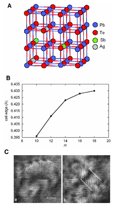
Figure 2 The difficulty of searching experimentally for the optimal high-ZT material is illustrated in this figure. AgPbmMTe2+m (where M is either Sb or Bi and m varies from 10 to 18) is a candidate for a high ZT material. What is the optimal composition? Fig. 2A shows the average ideal crystal structure; repeated x-ray diffraction experiments indicate that the lattice constant varies with m for M=Sb, as shown in Fig. 2B. But TEM reveals that the x-ray diffraction has not detected the presence of nanodots of differing composition in Fig. 2C.
Nanoscale thermoelectric materials that can independently reduce phonon transport without deteriorating electronic transport have been implemented in Bi2Te3/Sb2Te3 superlattices offering a ZT of ~2.4 at 300K and quantum-dot PbTe/PbTeSe superlattices offering a ZT of ~2 at 550K. Most of the enhancements have been attributed to lattice thermal conductivity reduction in nanoscale dimensions. It is anticipated that further reduction is possible with a comprehensive understanding of phonon transport in low-dimensional systems. There is also potential for significant ZT enhancement through quantum-confinement effects .
Thermophotovoltaics
Significant progress has been made in the TPV cells. The efficiency of TPV systems depends critically on the spectral control so that only useful photons reach the PV cells. Ideally, spectral control should be done at the emitter side, although filters standing alone or deposited on PV cells are also being developed. However, the temperature of the emitters exceeding 1,000°C imposes great challenges to the stability of the materials and structures used in a TPV system, especially for those components that provide spectral control.
Solar Concentrators and Hot Water Heaters
Today’s concentrators generally consist of a precise shaped metallic support structure and silverglass reflector elements with an average reflectivity of 88%. They are responsible for more than 50% of the investment costs of concentrating solar systems. Likewise, the primary challenge for widespread implementation of nonconcentrating solar thermal energy is to substantially reduce the initial cost of installed systems. Future research should aim at a paradigm shift from metal/glass components to integrated systems manufactured using mass production technique, such as those associated with polymeric materials. Major limitations of currently availably polymers are outdoor durability (UV; water, oxygen, mechanical stress, thermal stress) for at least 20 years. Needs include development of thin-film protection layers for reflectors, high strength, high thermal conductivity polymers; development of materials with high transparency and durable glazing for heat exchangers, and engineered surfaces that prevent dust deposition on reflector surfaces.
Thermal Storage Materials
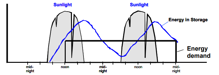
Innovative thermal storage methods must address the need to provide reliable electricity supply based on demand, which generally does not coincide with the incident sunlight periods, as demonstrated in Figure 3. Achieving this requires the development of high energy density, high thermal conductivity, and stable, latent heat materials for thermal storage. One promising approach is using encapsulated and nanocrystal polymers.
The operating conditions (i.e., temperature and pressure) of the thermal storage must match those of the power conversion process, and therefore, vary from 80–150°C for low-temperature systems and 400–1,000°C for high-temperature systems. Solar-derived fuels become the logical choice for storage at >1,000°C.
SCIENTIFIC CHALLENGE
Theoretical Methods to Identify Photovoltaic Materials with Targeted Properties
Currently, theoretical tools exist that enable first-principles calculation of total-energy and ground state electronic structure (e.g., density functional theory), but such methods are computationally very expensive. Even more expensive is accurate calculation of electronic excited states using, for example, quantum Monte Carlo methods. Thus, first-principles theoretical treatment of systems with many more than 1,000 atoms is currently beyond practicality for most systems. Thus it is not practical to use first-principles methods to exhaustively calculate the atomic and electronic structure of all possible photovoltaic materials. Methods that could circumvent this limit would be those that enable property-based identification of promising candidate materials and then subsequently calculate electronic structure of a restricted set of chosen materials (see Figure 4). Methods to select candidates might include cluster variation-based methods and simulated annealing, genetic algorithms, among others.
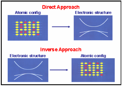
Figure 4 Inverse electronic structure calculations. In the direct approach, the modeler starts with a given atomic configuration and calculates the electronic structure. In the inverse approach, the modeler is told the electronic structure and must search to find an atomic configuration that will produce an electronic structure close to the one required. The inverse approach is a more difficult challenge.
High-throughput Experimental Screening Methods for Discovery of Designed Materials
Determining the suitability of materials for photovoltaics is currently not a systematic process. For example, one of the most widely used semiconductors for this is of photovoltaic cells is copper-indium/gallium-diselenide (CuxGa1-xInSe2). It was unexpectedly discovered that smallarea CuxGa1-xInSe2 cells work very well, despite being polycrystalline and containing many point defects, because sodium diffuses from glass substrates into the CuxGa1-xInSe2 film, interacts with grain boundaries, and reduces recombination. Had the initially undesired sodium diffusion not occurred, it is not clear that CuxGa1-xInSe2 technology would have reached its current state of development. This example points out the importance of experimentally testing films with many combinations of elements, even if there is no underlying heuristic or formal theoretical prediction suggesting that such combinations might have desirable properties. Since there are enormous numbers of alloy compositions to try, high-throughput screening methods are needed. Furthermore, promising polycrystalline thin-film solar cells based on CdTe and CuInSe2 are dramatically affected by the grain structure resulting from growth on foreign substrates, intentional and/or unintentional doping by impurities, the nature of the active junction, and ohmic contacts; all these processes and effects are poorly understood. A basic understanding of these issues would facilitate a revolutionary advance in the performance and economic viability of polycrystalline thin-film PV.
A big research challenge here is to find appropriate and efficient tests of specific photovoltaic properties that enable testing for millions of material combinations. Materials synthesis is often not itself the bottleneck in an approach, owing to relatively straightforward vapor deposition methods for multiple source deposition of elements to form compounds; the more difficult challenge is often to develop experimental methods for properties-based materials selection. As an example, the energy band gap of the materials could quickly be determined by measuring the absorption spectrum. Some information on the rate at which recombination occurs could be determined by measuring the photoluminescence efficiency. Conceivably, arrays of solar cells could be made to directly determine quantum efficiency, fill factor, and open circuit voltage; in this case, contact-less methods for properties measurements would be highly desirable. Pumpprobe spectroscopic techniques could be used to determine the cross-section for impact ionization (multiple electron-hole pair generation). Ideally, such screening methods will identify good candidates for more thorough photovoltaic testing.
Thermoelectrics
Fundamental Understanding of Nanoscaled Inclusions in Bulk Materials. Nanoengineered bulk materials may indeed be a key to achieving high-performance bulk thermoelectric materials. Understanding the role and stability of the interface between the nanomaterials and the matrix is essential in order to effectively optimize the materials. An effective interface must be thermally stable and promote electron transport while impeding phonon transport. Interface issues such as diffusion and segregation processes, doping and composition of the nanostructures, differential thermal expansion, and chemical contrast are essential for investigation.
Role of Interfaces in Nanocomposite Materials. Experimentally obtained improvements in ZT in two superlattice structures benefited mainly from reductions on the phonon thermal conductivity. A further increase in ZT in a wide range of structures and materials is possible by engineering phonon transport through interfaces. For example, it has been demonstrated experimentally that the phonon thermal conductivity of superlattices can be significantly smaller than the theoretical minima of their constituent bulk materials. Modeling suggests that it is the incoherent superposition of interface reflection of phonons that is the major cause of phonon thermal conductivity reduction . However, phonon reflection and transmissivity at single interfaces cannot be predicted at this stage, except at very low temperatures.
Electron Transport in Nanoscale Materials. While there has been significant attention paid to phonon transport in nanoscale systems, only a limited study of electronic transport in nanoscale thermoelectric materials and structures has been conducted. Significant opportunities exist for fine-tuning in two-dimensional superlattices to optimize the mini-band conduction as well as obtain a delta function in DOS. A major development in itself could be the general theory of electronic transport in solid state materials, with ZT >1, where isothermal conditions cannot be assumed during current flow. A new theoretical framework needs to be developed in the study of solid-state thermoelectrics, where quantum effects, multi-valley effects, strain-induced band-gap engineering effects, sharp DOS, and nonisothermal electronic transport are all brought into play. Theoretical and experimental methodologies to determine these quantities should be developed.
Thermophotovoltaics
We need to gain a basic understanding of novel materials for spectral control. Photonic crystals, plasmonics, phonon-polaritons, coherent thermal emission, left-handed materials, and doping with lanthanides are concepts from the optics community that can be exploited for the spectral control components required in TPV systems. Insight has to be gained into fundamental processes, such as emission.
Nanostructured Metallic and Dielectric Materials with Low Diffusion and Evaporation Rates. The major challenge of spectral control for TPV systems is given by the high operating temperatures of ∼1,200°C in fuel-powered TPV and ∼2,000°C in solar TPV. Diffusion processes and evaporation of material may limit the durability of the components significantly. Suitable concepts of material engineering to reduce theses effects have to be developed and fully understood by using multiscale models.
Scalable Manufacturing Processes Applicable to Various Geometries. The optical approaches mentioned are based on materials properties and on precise nanostructuring of the materials. The techniques for producing nanostructures are top-down approaches that are limited to small, homogeneously structured areas and to flat surfaces nowadays. They are also not costefficient. Thus, novel techniques have to be developed, which very likely incorporate selforganization processes.
Solar Concentrators and Hot Water Heaters
Heat transfer surfaces for water heaters call for polymer/composites with high mechanical strength, UV degradation resistance, high thermal conductivity, and concentrator support structures requiring polymers with high mechanical strength and a low thermal expansion coefficient. The thermal conductivity of most polymers is 0.2 to 0.4 W/m-K. An order-ofmagnitude increase in thermal conductivity is needed to make polymers competitive. New composite materials hold the promise of high mechanical strength and high thermal conductivity.
Surface modifications are needed for photon and thermal management. High-efficiency solar absorbers for water heaters can explore the concept of photonic crystals. Mirrors and glass that are dirt repelling can significantly increase efficiency and reduce cleaning cost. Surface engineering is also needed to prevent scale formation in solar thermal heat exchangers. Fundamental research on particle-surface interactions and solid precipitation and deposition processes can help solve these challenges.
Thermal Storage Materials
Fundamental understanding of the behavior of phase change storage materials (PCM) and the relationship between various (sometimes undesirable) chemical processes, phase transition, and thermal/chemical stability are crucial for the development of thermal storage. These materials must have high latent heat density (>0.3 MJ/kg) and sufficiently high thermal conductivity for enhanced thermal energy charge/discharge processes. Encapsulation of “pockets” of PCM is a possible approach to improve thermal energy transport, while maintaining the chemical and mechanical stability of the material. Recent developments of nanocrytstal polymer composites can be the key to a stable cycling solution for thermal storage.
The unique characteristics of solid-solid structural transformations in nanocrystals can lead to a new generation of thermal storage materials. Present thermal storage materials are limited by the lack of reversibility of structural transformations in extended solids. In contrast, nanocrystals embedded in a “soft matrix” can reversibly undergo structural transitions involving a largevolume change per unit cell. This is because a structural transition in a nanocrystal may proceed through a single nucleation event per particle (see Figure 5). Further, a nanocrystal can change shape and volume without undergoing fracture or plastic deformation. In addition, the barrier to a structural transition depends strongly on the size of the nanocrystals so that the hysteresis and kinetics of the structural transition can be controlled. Much of the prior work on structural transitions in nanocrystals has focused on pressure-induced transitions, or transitions that occur at modest temperatures (a few hundred degrees Celsius), so exploratory work must be performed to find materials and transitions that will perform thermal storage under the appropriate conditions for solar thermal.
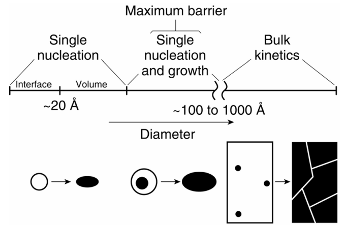
Figure 5 Illustration of various size regimes of the kinetics of solid-solid phase transitions. Defects, which act as nucleation sites, are indicated by asterisks in the cartoon of the bulk solid.