Temperature acquisition circuit design and its principle
Circuit Design Principle
As the power generation process needs to measure and control nearly 40 groups of temperature parameters at the same time, it needs multiple K-type thermocouples to measure the temperature of each temperature measurement point at the same time. Multiple K-type thermocouples output mV-level weak signals, which are amplified by amplifiers, and then the analog-to-digital conversion circuit converts the amplified analog signal into a digital signal and transmits it to the microcontroller through the parallel port.
Signal amplification circuit
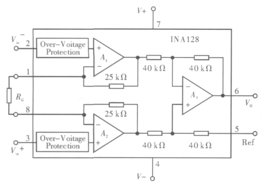
Since the K-type thermocouple measures temperature based on the thermoelectric potential generated by the temperature difference between the hot and cold ends, its output is a small signal of mV level, and the AD7606 is a ±5 V bipolar signal input, so if the small signal of mV level is to be converted into a digital quantity by the AD7606, it must be amplified precisely first. The INA128 instrumentation amplifier is selected as the preamplifier for this circuit. k-type thermocouple output mV level small signal, easy to be measured by the noise interference around the environment, so the signal path of other electronic components have high requirements. Therefore, the INA128 is selected as a precision low-power instrumentation amplifier with differential input characteristics, high common-mode rejection ratio and small temperature drift, which can effectively reduce noise interference, and its internal principle circle is shown in Figure 3. Its internal principle circle is shown in Figure 3. It integrates 3 pieces of OP amplifier with small package size, which makes its application range quite wide. Its amplification can be adjusted from 1 to 10 000, and the external only needs to be adjusted by connecting a resistor, and its amplification G=1+50 kQ/RG.
The amplifier circuit uses a 680Q precision resistor, which results in an amplification factor of G= 1 + 50 kQ/RG=74.5. This is because the range of the thermoelectric potential generated by a K-type thermocouple is between – 555 mV based on the temperature difference between the hot and cold ends, and the amplified analog voltage range must be within ±5 V of the analog signal input range of the AD7606. The 680 2 precision resistor can better meet the above requirements. The schematic diagram of the amplifier circuit is shown in Figure 4, TA1- and TA1+ are connected to the induced thermodynamic output of the K-type thermocouple, and the analog signals between TA1N and TA1P are the amplified signals, which are connected to the differential analog signal input of the AD7606 for A/D conversion.
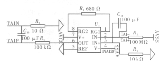
It is important to note that the circuit incorporates a break-couple detection function. Figure 4, TA1- through a large 100 MQ resistor connected to Avss ( -5 V), where the large resistor to play a current-limiting protection, when the K-type thermocouple is disconnected, that is, between TA1 – and TA1 +, the voltage at TA1 – is AVss ( -5 v), TA1 + ground (O V), that is, the INA128 input stage voltage is 5 V The amplified voltage of INA128 is 5 V, and the thermodynamic potential of K-type thermocouple ranges from -555 mV to a maximum of 4.1 V after amplification by INA128, thus determining whether the thermocouple is disconnected. The disconnection detection function greatly facilitates the determination of thermocouple installation for poor contact and detection of thermocouple damage.
A/D conversion circuit
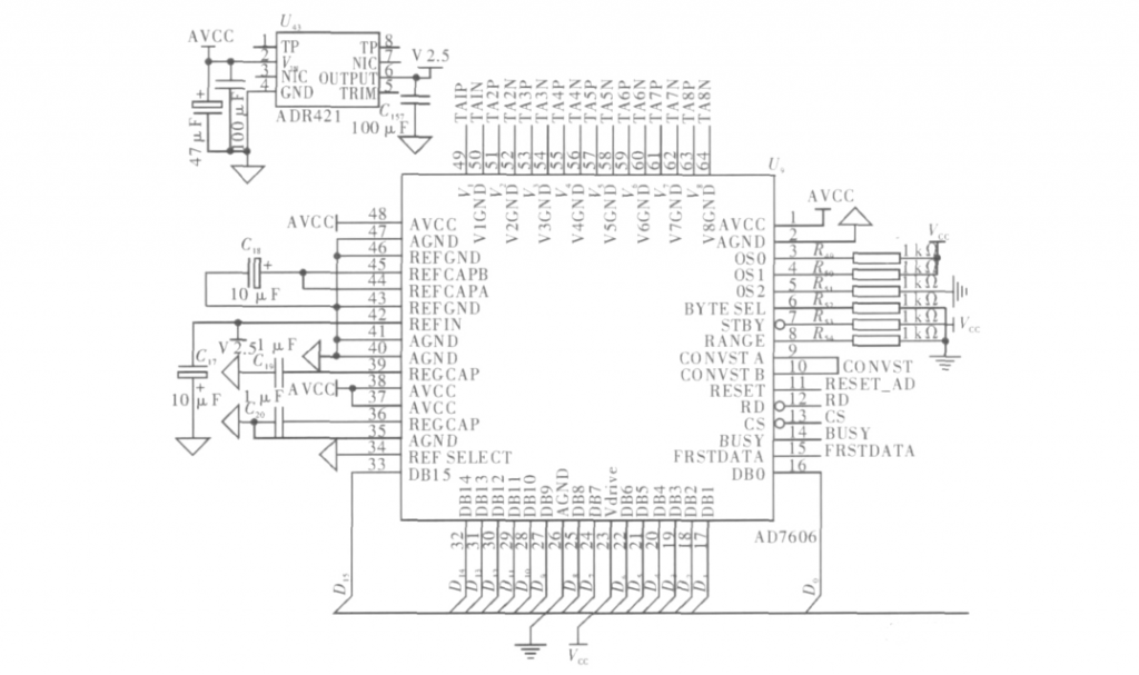
The A / D converter circuit is based on the 16-bit 8-channel synchronous sampling A / D converter chip AD7606. Since many groups of temperature data need to be measured, and each AD7606 can collect 8 groups of temperature, so the 8-channel AD7606 can effectively reduce the size of the finished circuit board, and its 16-bit resolution can make the temperature measurement accuracy reach 0.1 ℃ to meet the project requirements. The AD7606’s synchronous sampling and adjustable sampling rate can ensure the sampling efficiency, and the AD7606 has two data transmission methods, serial and parallel port, using 16-bit high-speed parallel port transmission method, which also significantly saves data transmission time and improves transmission efficiency, thus saving more time for the host microcontroller to improve its own execution efficiency.
The AD7606 has an internal 2.5 V bandgap voltage reference and a reference buffer circuit with a typical temperature coefficient of ±10 x 10 -/c. When designing the circuit, either the internal integrated 2.5 V bandgap voltage reference or an external reference can be selected. Because, solar generator equipment is mainly installed in areas with strong light and abundant solar energy, these areas usually have a large temperature difference between day and night, which requires a high voltage reference, and the temperature drift of the AD7606 internal integrated voltage reference is large, which does not meet the requirements. In addition, when using multiple ADCs at the same time, if high absolute accuracy is required, an external reference with high initial accuracy and low temperature coefficient should be used to eliminate the error caused by the difference between the built-in references of different devices. The circuit is selected with an initial accuracy of 0.04%, a temperature coefficient of 3 × 10-/°C, and a voltage of 2.5 V. The reference chip ADR421 is used as the external reference source, The schematic of the A/D converter circuit is shown in Figure 5. In the figure, the OSC2:O pin of AD7606 sets the chip sampling rate to 25 ksample- s ‘The REF SELECT pin is set to external reference voltage, the BYTE SEL pin is set to high-speed parallel port, the RANGE pin is set to the chip’s analog input range of ±5 V, and the 4964 pin is a differential analog input pin, which is connected to the analog signal amplified by INA128.
Experiment and conclusion
In the experiment, the millivolt voltage source is connected to the input of INA128 instead of the K-type thermocouple, which simulates the thermal potential generated by the K-type thermocouple, and the power supply provided by the power supply board is connected to make the sampling circuit work normally. The output voltage value (Vn between TA1 – and TAl +) of the millivolt voltage source is adjusted, and then the output voltage value (VouT between TA1N and TA1P) of the INA128 is measured after amplification, and the AD value obtained after analog-to-digital conversion of the AD7606 is read out by the online debugging function of the microcontroller.
| VIN/mV | VOUT/V | AD values |
| -0.5 | -0.38 | -2 236 |
| 0.0 | 0.02 | 4 |
| 5.0 | 0.38 | 2 241 |
| 10.0 | 0.75 | 4 473 |
| 15.0 | 1.12 | 6 683 |
| 20.0 | 1.50 | 8 908 |
| 25.0 | 1.87 | 11 117 |
| 30.0 | 2.23 | 13 356 |
| 35.0 | 2.60 | 15 578 |
| 40.0 | 2.97 | 17 815 |
Table 1 shows the change of the voltage value Vou, between TA1N and TAIP, and the change of the AD value obtained after A/D conversion when the voltage value Vr, between TA1- and TA1+, changes. Observing the change rule between them, we can conclude: First, no matter how V, changes will cause the change of VouT, and the value of Vour is always about 74.5 times of the value of V, which shows that the INA128 amplification error is small, high precision, and ideal amplification effect. Secondly, the change of Vou, also causes the change of AD value, and the change law of both is almost identical, and equal proportional change, which shows that the AD7606 has high resolution, small gain error and offset error when A/D conversion, and the converted digital quantity is correct and stable, and can be used for operation.
During the experiment, we also verified the effect of ambient temperature change on the working condition and conversion accuracy of AD7606. The input voltage Vy was selected arbitrarily, and the AD value obtained from the AD7606 after analog-to-digital conversion was recorded when the ambient temperature of the AD7606 was changed by a hot air blower, and the changes were observed as shown in Table 2.
| VIN/mV | ~3℃ | ~20℃ | ~40℃ |
| 6.5 | 2 899 | 2 907 | 2 913 |
| 16.4 | 7 307 | 7 315 | 7 313 |
| 36.9 | 1 6434 | 16 441 | 16 436 |
| 50.3 | 2 2405 | 22 401 | 22 411 |
As shown in Table 2, the AD value obtained from the AD7606 after analog-to-digital conversion remains the same when the ambient temperature is changed. Therefore, the AD7606 works stably and has high conversion accuracy when the external reference is selected, and is almost independent of the ambient temperature. Thus, it can be concluded that the ADR421 is suitable for the reference voltage source of the AD7606 because it is less affected by the temperature, and the design of the AD7606 with external reference is successful.